IoT
Edge AIVoice Control
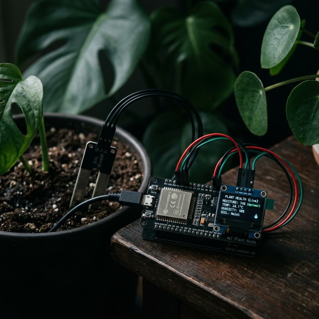
SmartPot — AI Plant Companion
Voice-controlled ESP32 plant assistant with edge AI and sensor intelligence.
ESP32FreeRTOSTensorFlow LiteMQTT
Firmware & AI Systems Engineer
View Details →The hex light panels and enclosures in my own projects came off my own bench and printer. Bring a sketch, a board or a broken part and we can test the fit together.
Built in Assam · Assam Engineering College alumnus
4+ Years
Building systems
Remote + Onsite (Guwahati Area)
Breadboard → PCB Prototype → Enclosure & Test Fit
Optimization Summary
Most prototypes stall at the same step: getting off the breadboard and into something that fits, survives and can be built again.
“The breadboard prototype works on the desk but fails when moved.”
A custom PCB with proper power rails, decoupling and connectors replaces loose wiring, so the circuit behaves the same every time.
“The board doesn't fit the enclosure.”
I export the routed board from KiCad as a 3D model and design the case around it in Fusion 360, so mounting holes, USB ports and LEDs line up.
“Printed brackets snap or warp under load or heat.”
Parts designed for printing: layer lines aligned with the load, thicker walls, and PETG or ABS where there is stress or warmth.
“LEDs flicker or the board resets when everything switches on.”
A power budget for the whole system, a supply sized for peak current, and power injection for long LED runs, as in my modular light panels.
For anyone with an idea, a breadboard or a broken part who needs a real, physical thing that works.
Founders whose prototype is a tangle of jumper wires and dev boards, and who need a compact board and case they can show, test and hand out.
Final-year projects, lab rigs and sensor mounts that have to survive real use, like the printed brackets on my 6-DOF robotic arm.
Small control boxes, display boards, replacement brackets and mounts that nobody sells, made without paying for moulds.
Looks-like and works-like prototypes to check size, weight, buttons and assembly before committing to manufacturing.
Working hardware, plus every file needed to make more of it.
Schematics, 2–4 layer board layouts and custom footprints, organised so changes are easy.
Gerbers, drill files, a BOM with LCSC/DigiKey part numbers, and pick-and-place files for assembly services.
Soldered, powered-up and tested boards, with firmware flashed where the project includes it.
Parametric Fusion 360 source, STEP files for manufacturers, and print-ready STL/3MF, plus the printed parts with brass inserts fitted.
Wiring, assembly order, print settings and a parts list, so someone else can build the next one.
The electronics and fabrication work I do most.
Microcontroller boards (ESP32 and others) with sensors, drivers, connectors and protection on one board, routed in KiCad and ready for fabrication.
Addressable LED builds with proper power distribution and custom firmware, like my audio-reactive modular hex light panels (WS2812B, FastLED).
Cases designed around the board, with vents, snap fits and threaded inserts, plus load-bearing brackets and joints like those in the SmartPot and the robotic arm.
Design tools, electronics building blocks and fabrication methods I use.
How I take a circuit from breadboard to a working board, and then design and print the enclosure around it: schematic and layout in KiCad, first power-up, and FDM parts modelled around the real PCB.
A breadboard proves the idea; a PCB makes it repeatable. Loose jumper wires add resistance, pick up noise and fall out when the prototype is moved. Moving to a custom board is where most of the reliability comes from, as long as a few rules are followed in the schematic and layout.
Decoupling Belongs at the Pin
Every microcontroller and sensor supply pin gets its own small ceramic capacitor (typically 100nF), placed as close to the pin as the layout allows, with a larger bulk capacitor near where power enters the board. A capacitor that is in the schematic but far away on the board does very little.
The checklist I apply before sending a board to fabrication:
Powering Long LED Strips from One End
Addressable LEDs like the WS2812B can draw up to around 60mA each at full white. Feeding a long run from one end makes the far LEDs dim and shift colour, and the voltage drop can reset the microcontroller. Inject power at several points, put a large capacitor across the supply, and add a small series resistor on the data line.
When the boards arrive, bring-up follows a fixed order: visual inspection for bridges and missing parts, a continuity check between power and ground, power on with a current-limited supply, measure every rail, and only then flash the microcontroller and test each peripheral one at a time. Problems found this way cost minutes, not a new board revision.
Traditional CAD modeling focuses on subtractive milling or injection molding. Prototyping casings using FDM (Fused Deposition Modeling) 3D printers requires Design for Additive Manufacturing (DFAM), adjusting parameters to account for layer lines, extrusion width, and plastic thermal shrinkage.
Clearances on Snap-Fits
Modeling interlocking parts (such as casing lids or snap joints) without clearances will result in parts fusing together or cracking. Standard FDM printers require a clearance threshold of 0.15mm to 0.25mm on mating surfaces to allow components to snap together smoothly without friction slips or loose fits.
When modeling physical casings for custom PCBs, I export the physical board models directly from KiCad and import them into Fusion 360. This guarantees that USB port cutouts, mounting pins, and LED indicators align precisely with routed components.
Below is the mechanical layout checklist I apply in Fusion 360 before slicing and printing casings:
Layer Line Alignment
Always align print orientations so that physical stress is perpendicular to layer lines. Since layers fuse together, parts are weaker along the Z-axis. Aligning joints along X and Y axes increases mechanical load capacity.
Slicing translates 3D models into G-code commands. Standard PLA plastic is fine for visual mockups but warps easily under sunlight or warm electronics. I optimize slicing parameters in PrusaSlicer/Cura and select high-durability filaments (PETG or ABS) for structural components.
Incorrect Infill Patterns for Load-Bearing Parts
A common mistake is using high infill density (e.g. 80% Grid infill) to make parts strong. This wastes filament and increases print time without improving strength. Instead, increasing the wall loop count (from 2 to 4 or 5) and selecting a Gyroid infill pattern (at 20-30% density) yields much stronger, lightweight parts.
  Naively Printed (Grid Infill)          Optimized DFAM (Gyroid Infill)
  +---------------------------+          +---------------------------+
  |  |  |  |  |  |  |  |  |   |          | ~ ~ ~ ~ ~ ~ ~ ~ ~ ~ ~ ~ ~ |
  |  |  |  |  |  |  |  |  |   |          | ~ ~ ~ ~ ~ ~ ~ ~ ~ ~ ~ ~ ~ |
  |  - High weight            |          | - Omni-directional load   |
  |  - Directional weakness   |          | - 30% lighter weight      |
  +---------------------------+          +---------------------------+
The NanoLeaf Modular Interconnects
During the development of the Lumex Nanoleaf System, panels had to lock together repeatedly. The first PLA prints broke easily at the joint clips. I redesigned the joints in Fusion 360 using a 0.2mm tolerance, switched the filament to PETG, and adjusted the slice orientation. This created sturdy snap-joints that survived thousands of assembly cycles.
To construct robust enclosures that can be disassembled for debugging, I avoid driving screws directly into plastic threads (which strip easily). Instead, I model pilot holes and heat-press brass threaded inserts (M2/M3) into the casing:
Prove the circuit, then the board, then the box.
Phase 1 of 8
We pin down inputs, outputs, power source, size limits and the environment it will sit in: heat, dust, damp or vibration.
Dynamic projects fetched from the portfolio database demonstrating execution.
Voice-controlled ESP32 plant assistant with edge AI and sensor intelligence.
Firmware & AI Systems Engineer
View Details →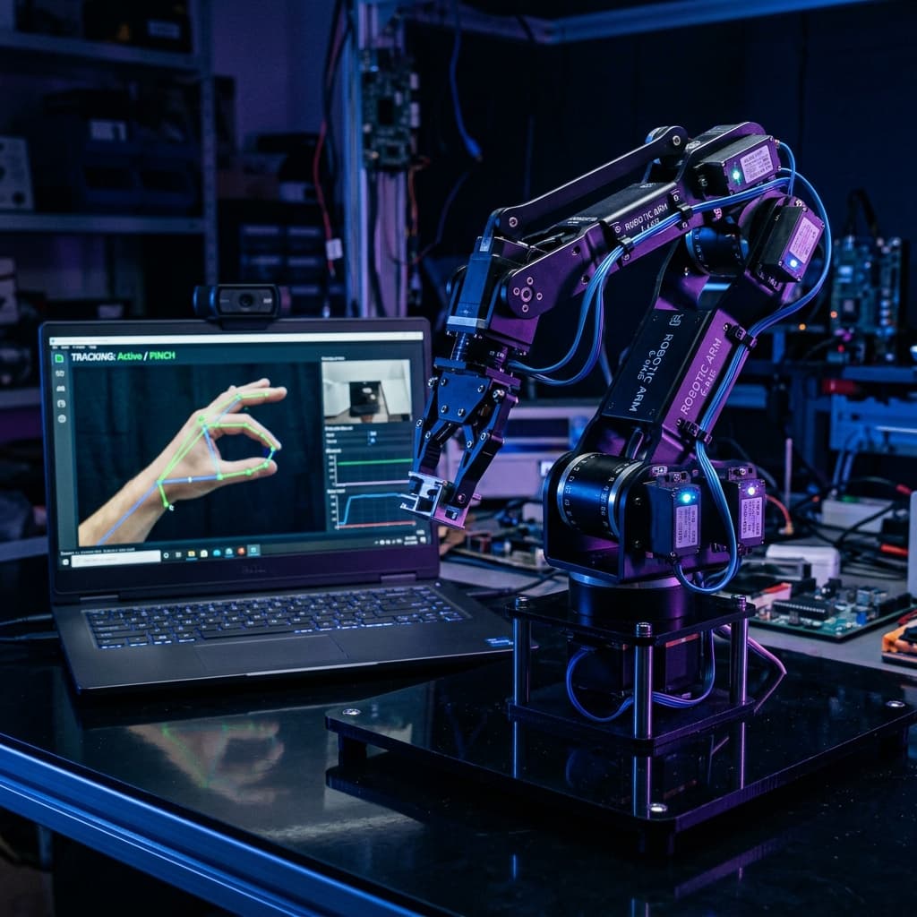
Gesture-controlled multi-axis arm with computer vision.
Firmware & System Engineer
View Details →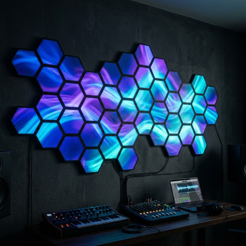
Audio-reactive modular lighting with custom firmware.
Embedded Engineer
View Details →When the PCB designer, firmware developer and print shop are three different people, most problems happen where their work meets. I do all three.
| What Matters | My Prototyping Service | Typical Print Shop or PCB Freelancer |
|---|---|---|
| Board + Enclosure Fit | ✓ Case modelled around the real KiCad board. | ❌ Separate people; fit issues found after printing. |
| Custom CAD from Scratch | ✓ Designed for your parts and use. | ⚠️ Print shops usually need a ready STL. |
| Working Firmware | ✓ Boards delivered powered up and tested. | ⚠️ Bare boards; bring-up left to you. |
| Durable Assembly | ✓ PETG/ABS where needed, brass inserts for screws. | ⚠️ PLA with screws straight into plastic. |
In Guwahati you can bring the hardware in person: we test fits on the spot, hand over prints directly and turn revisions around in days.
For clients elsewhere in India (Bengaluru, Hyderabad, Pune, Mumbai, Delhi NCR) and abroad, I share 3D models and bring-up videos as we go, and ship boards and parts by courier.
Structured query answers targeting specific informational searches.
Send a sketch, a breadboard photo or a broken part. I'll tell you what it takes to turn it into a working board and enclosure.